Microfluidics Automation: Robotics
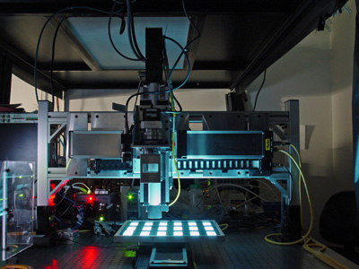
I developed a tool that is capable of serially interfacing &
manipulating a set of PDMS-based substrates. The tool is comprised of a set of micron-
precision translation stages, a custom-designed injector/interface module, a vision system, and
a set of solenoids for flow control. Custom software written in LabWindows CVI is used to
coordinate the various components. While the initial scope of this tool was to automate the DNA
flow-patterning process that is used to create custom assay substrates within our group, minor
modification will allow it to perform any PDMS-based experiment that is normally done by hand.

DNA Microarray Patterning
With the development of the DEAL technique, our lab abandoned
electronic sensing in favor of colorimetric, ELISA-type assays. ELISA assays are commonly
considered the gold standard for protein detection, but typically require relatively large amounts
of reagent & analyte. The DEAL technique allowed us to transform standard DNA microarrays into
antibody microarrays, where each unique DNA spot becomes sensitive to a specific protein. This
enables us to run hundreds of ELISA-type protein detections in parallel and within a relatively
small space, allowing for drastically reduced reagent and analyte volumes among other advantages.
I worked extensively on methods to create second generation microarrays with more flexible spot
size and morphology than commercially-available products, with the ultimage goal of further
reducing reagent requirements and enabling new classes of experiments.
Microcontact Printing
Microcontact printing utilizes PDMS as a physical stamp: extruded
features are inked with molecules of interest and then brought into contact with the surface to
be patterned. Single-stranded DNA is an ideal ink for such a process, as it initially adheres
well to PDMS through hydrophobic interactions but then transfers efficiently to postively-charged
substrates (aminated or poly-lysine slides) via electrostatic interactions. After an initial
demonstration of the transfer process I was quickly able to reduce feature size by an order of
magnitude (as compared to traditional microarrays) and incorporate arbitrary spot morphology. I
also solved numerous technical issues associated with the process that are critical if such
microarrays are to be used for subsequent experiments. Chief among these was aligning multiple
stamps to a single substrate with micron precision such that each DNA spot/sequence can be located
reliably relative to its neighbors; a standard Karl Suss MA6 was adapted to accomplish this goal.
Moreover, I developed a technique to print extremely low-aspect-ratio features at any distance
from one another without intermediary support structures, overcoming a common problem in the
field known as "roof collapse". Microcontact printing ultimately proved to be incompatible with
DEAL chemistry due to monomer contaminants left behind by the stamping process.

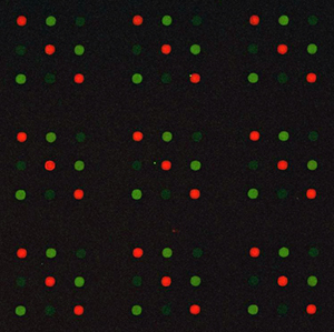
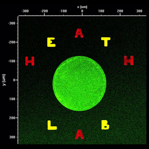
a traditional 3-element DNA microarray with 150um spot size

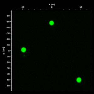
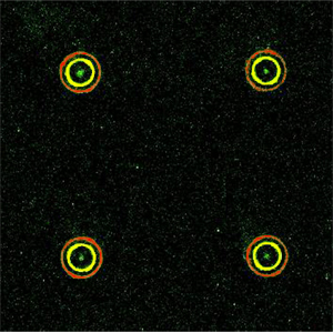
10um fluorescent DNA spots generated by microcontact printing

fluorescent image demonstrating flexible spot morphology and alignment
Microfluidic Flow Patterning
In spite of a disappointing end to the microcontact printing
project, the specific failure mode - substrate surface contamination - inspired a new approach
to generating DNA microarrays. Indeed, the process of microfluidic flow patterning represents
the exact inverse of microcontact printing: here a flat PDMS mold is placed onto a substrate with
cavities/channels (rather than extrusions) at the spots that are to be patterned. A DNA solution
is introduced into the features and allowed to evaporate, depositing DNA in the shape of the
channel while relegating any contaminants to the spaces in between. With the introduction of
2-layer microfluidics with crossover channels, multiple discontinuous features could be patterned
in a single step. This approach proved to be compatible with DEAL chemistry and serves as the
basis for all of the high-denisty DEAL assays performed in the Heath Lab today, including blood
analysis and single-cell secretion experiments.

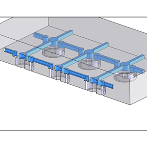
concept sketch of a microfluidic mold for flow patterning discontinuous features

3-protein assay on a flow-patterned DNA microarray with discontinuous features

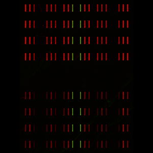
barcode microarray with 20um-wide bars generated by flow patterning
Silicon Surface Functionalization
A critical component of electrical sensing with Si nanowires is
decorating the Si surface with capture agents that will spatially localize specific analytes of
interest to the wire. Using fluorescence-based assays, I found that our existing strategies for
covalent surface modification were relatively inefficient and yielded poor surface coverage of
our sensors. I explored alternative methods of covalently functionalizing Si surfaces with
higher efficiency and with spatial selectivity.

Protein Sensing with Silicon Nanowires
Silicon is an extremely common, relatively cheap semiconductor
material that is ubiquitous in today's electronics. The explosive growth of the computer industry
over the past two decades spurred comprehensive study of the material, and the processing
techniques used to create Si-based devices are very well characterized today. If Si could be
configured as a chemically-gated Field Effect Transistor (FET), it would integrate seamlessly with
today's electronics, providing a relatively cheap, compact, high-throughput method of exploring the
biological molecules that underlie a wide variety of diseases. We chose to use nanowire structures
for our FET sensors because the high ratio of surface area/volume inherent to nanowires renders
them significantly more sensitive to local field effects. Under the guidance of postdoctoral
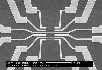
scholars Peter Willis & Kristen Beverly, I investigated both DC & impedance detection methods on ca.
25nm wires defined by e-beam lithography. The project bore robust results for simple systems (e.g.
biotin/streptavidin binding in low-salt buffers) but failed to yield convincing data with more
complex analytes.
